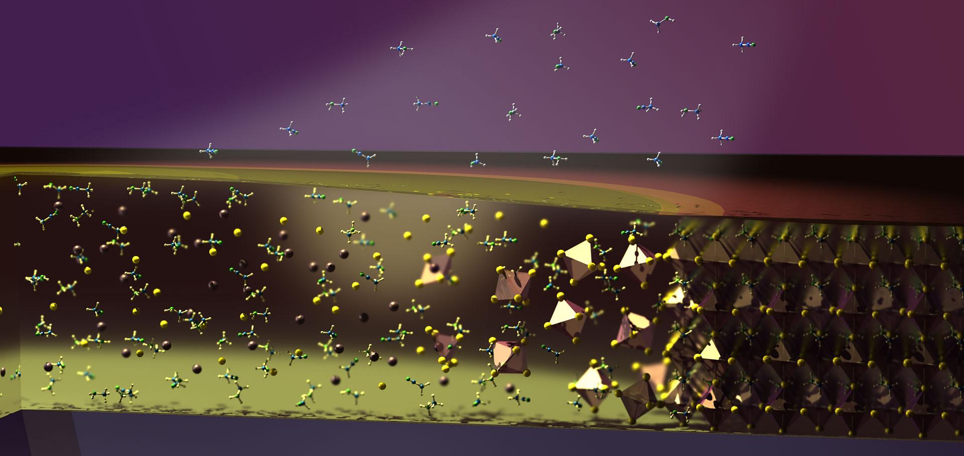
Odd–Even Cation Engineering of the Excitation Transport Anisotropy in Two-Dimensional Perovskite Films
ACS Nano American Chemical Society (ACS) (2026)
Abstract:
Two-dimensional perovskites have emerged as promising materials for optoelectronic applications owing to their excellent environmental stability and tunable quantum confinement. Such 2D perovskites can incorporate a particularly versatile range of organic cations of different size, chemical nature, and optoelectronic character. However, understanding and controlling thin-film transport for this vast family of materials remains a key challenge to their successful application in devices. Here, we systematically investigate odd-even effects in thin films of Ruddlesden-Popper-type (RP) lead-iodide 2D perovskites based on nonconjugated alkylammonium spacer cations with chain lengths ranging from three to eight carbon atoms. A pronounced odd-even dependence on the carbon number is observed in both optical and transport properties, including absorption coefficients, photoluminescence energies and lifetimes, and excitation diffusion dynamics. Notably, the coefficients for charge-carrier diffusion out of the film plane─extracted via a dynamic photon reabsorption approach─display an opposite odd-even trend to the in-plane charge-carrier mobility obtained from optical pump-terahertz probe measurements, causing a pronounced odd-even modulation of the thin-film mobility anisotropy. Grazing-incidence wide-angle X-ray scattering measurements reveal that this behavior is related to cation-controlled nanostructural orientation: even-numbered alkyl spacer cations induce lead-iodide planes lying highly oriented within the film plane, while odd-numbered ones cause more disordered stacking. Furthermore, the observed 1/d2-dependence on interplane distance d in ordered films demonstrates that Förster resonance energy transfer underpins diffusion of excitations between lead-iodide layers. Our findings establish a direct structure-transport correlation in 2D perovskite films and provide valuable guidelines for the design of optoelectronic devices.Tracking the Breakdown of Quantum Confinement during Structural Degradation of FAPbI3.
The journal of physical chemistry letters (2026)
Abstract:
Bulk formamidinium lead triiodide (FAPbI3) films host spontaneously formed quantum-confined (QC) domains, but their structural origin remains unclear. Using controlled material degradation in humid air as a dynamic lattice perturbation, we track the evolution of QC features in thin-film absorption of FAPbI3. With aging, above-bandgap QC features redshift and diminish, indicating weakened electronic confinement. Concurrently, X-ray diffraction reveals that breakdown of α-phase connectivity coincides with the loss of short-range higher-order hexagonal (nH, n > 2) polytypes as the material converts to the 2H δ-phase. Such polytypic nanodomains may generate peaked absorption features by forming higher-energy barriers confining charge carriers within α-FAPbI3 or by introducing distinct electronic states associated with mixed octahedral connectivity. Progressive degradation dismantles this framework, causing the disappearance of the QC features. Our results identify the structural motifs underpinning QC effects and propose that controlling higher-order (n > 2) hexagonal polytypes offers a route to tuning quantum confinement in FAPbI3 films.Is Photoluminescence Spectroscopy a Suitable Probe of Halide Segregation?
ACS Energy Letters American Chemical Society (ACS) (2026)
Abstract:
Mixed-halide perovskites exhibit ideal band gaps for use in perovskite-based multijunction photovoltaics, but stable performance is compromised by light-induced halide segregation. Photoluminescence (PL) tracking is universally used to monitor such photoinstability; however, here we reveal that such data do not accurately quantify halide segregation. We utilize a combination of simultaneously recorded PL and X-ray diffraction (XRD) measurements to explore CH3NH3Pb(I1–x Br x )3 films across 18 different halide ratios. While PL data suggests that segregation rates increase exponentially with bromide fraction x, XRD patterns reveal that they are actually unchanged. We demonstrate that PL cannot accurately reflect the rate and extent of halide segregation because it is governed by charge funneling to iodide-rich minority domains, which is strongly influenced by additional factors, including luminescence efficiency, band energetics, and charge extraction. To assess the efficacy of treatments to suppress such photoinstabilities, it is therefore essential to probe changes across the full material volume, e.g. by monitoring XRD or absorption spectra.From precursor to performance: the impact of FAI impurities on halide perovskite thin films and devices
EES Solar Royal Society of Chemistry (2026)
Abstract:
While metal halide perovskites have yielded remarkable power conversion efficiencies in photovoltaic applications, uncertainty concerning their long-term stability remains a significant barrier to widespread deployment. Previous studies have demonstrated that trace impurities present in perovskite precursor materials can influence the crystallisation dynamics of perovskite thin-films and hence, affect crystal structure, film morphology and optoelectronic properties. However, the nature of the impurities in formamidinium iodide (FAI) and their effect(s) on film quality and device performance remain underexplored. In this work, we carry out a detailed analysis of the impurities present in commonly used commercial FAI sources, and probe their impact on the composition, structure, and optoelectronic quality of the resulting perovskite thin-films and devices. We find that while some FAI impurities can improve the optoelectronic properties of solution-processed perovskite thin-films, in vapour-processed films, their presence alters the sublimation behaviour of FAI, favouring irreversible degradation pathways which lead to the formation of sym-triazine. While sym-triazine does not directly incorporate into the perovskite films, the impurity-driven variation in sublimation behaviour results in films which can deviate from the target stoichiometry, even under otherwise optimised conditions; and thus, do not fully convert into the desired photoactive phase, eventually causing poor material stability. Our results highlight the importance of understanding and controlling impurity concentrations in perovskite precursor materials as a route to enhancing both performance and process reproducibility in perovskite solar cells.Crystal-facet-directed all vacuum-deposited perovskite solar cells
Nature Materials Springer Nature (2026)