Search for pair-produced higgsinos decaying via Higgs or 𝒁 bosons to final states containing a pair of photons and a pair of 𝒃-jets with the ATLAS detector
Abstract:
A search is presented for the pair production of higgsinos 𝜒˜ in gauge-mediated supersymmetry models, where the lightest neutralinos 𝜒˜ 0 1 decay into a light gravitino 𝐺˜ either via a Higgs ℎ or 𝑍 boson. The search is performed with the ATLAS detector at the Large Hadron Collider using 139 fb−1 of proton–proton collisions at a centre-of-mass energy of √ 𝑠 = 13 TeV. It targets final states in which a Higgs boson decays into a photon pair, while the other Higgs or 𝑍 boson decays into a 𝑏𝑏¯ pair, with missing transverse momentum associated with the two gravitinos. Search regions dependent on the amount of missing transverse momentum are defined by the requirements that the diphoton mass should be consistent with the mass of the Higgs boson, and the 𝑏𝑏¯ mass with the mass of the Higgs or 𝑍 boson. The main backgrounds are estimated with data-driven methods using the sidebands of the diphoton mass distribution. No excesses beyond Standard Model expectations are observed and higgsinos with masses up to 320 GeV are excluded, assuming a branching fraction of 100% for 𝜒˜ 0 1 → ℎ𝐺˜. This analysis excludes higgsinos with masses of 130 GeV for branching fractions to ℎ𝐺˜ as low as 36%, thus providing complementarity to previous ATLAS searches in final states with multiple leptons or multiple 𝑏-jets, targeting different decays of the electroweak bosons.Contrasting Ultra-Low Frequency Raman and Infrared Modes in Emerging Metal Halides for Photovoltaics
Abstract:
Lattice dynamics are critical to photovoltaic material performance, governing dynamic disorder, hot-carrier cooling, charge-carrier recombination, and transport. Soft metal-halide perovskites exhibit particularly intriguing dynamics, with Raman spectra exhibiting an unusually broad low-frequency response whose origin is still much debated. Here, we utilize ultra-low frequency Raman and infrared terahertz time-domain spectroscopies to provide a systematic examination of the vibrational response for a wide range of metal-halide semiconductors: FAPbI3, MAPbI x Br3–x , CsPbBr3, PbI2, Cs2AgBiBr6, Cu2AgBiI6, and AgI. We rule out extrinsic defects, octahedral tilting, cation lone pairs, and “liquid-like” Boson peaks as causes of the debated central Raman peak. Instead, we propose that the central Raman response results from an interplay of the significant broadening of Raman-active, low-energy phonon modes that are strongly amplified by a population component from Bose–Einstein statistics toward low frequency. These findings elucidate the complexities of light interactions with low-energy lattice vibrations in soft metal-halide semiconductors emerging for photovoltaic applications.Bandgap-universal passivation enables stable perovskite solar cells with low photovoltage loss
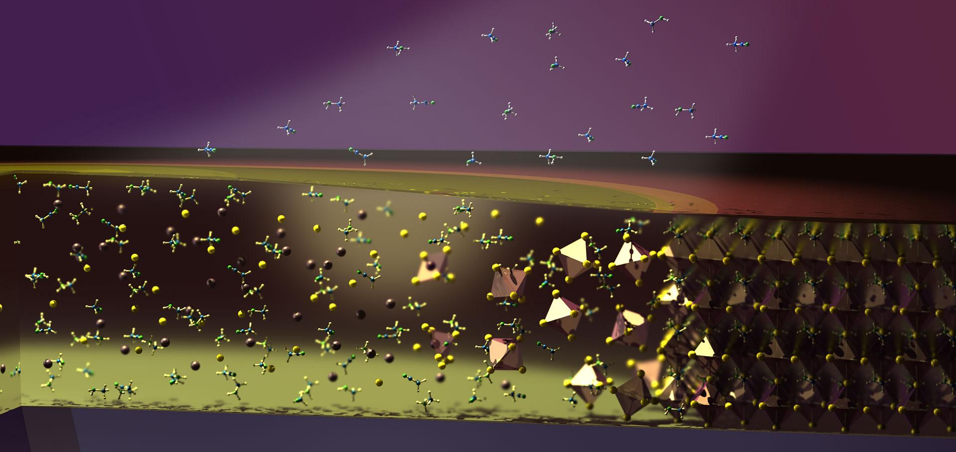
Abstract:
The efficiency and longevity of metal-halide perovskite solar cells are typically dictated by nonradiative defect-mediated charge recombination. In this work, we demonstrate a vapor-based amino-silane passivation that reduces photovoltage deficits to around 100 millivolts (>90% of the thermodynamic limit) in perovskite solar cells of bandgaps between 1.6 and 1.8 electron volts, which is crucial for tandem applications. A primary-, secondary-, or tertiary-amino–silane alone negatively or barely affected perovskite crystallinity and charge transport, but amino-silanes that incorporate primary and secondary amines yield up to a 60-fold increase in photoluminescence quantum yield and preserve long-range conduction. Amino-silane–treated devices retained 95% power conversion efficiency for more than 1500 hours under full-spectrum sunlight at 85°C and open-circuit conditions in ambient air with a relative humidity of 50 to 60%.