Structural chirality and natural optical activity across the α to β phase transition in SiO2 and AlPO4 from first principles
Journal of Applied Crystallography International Union of Crystallography (IUCr) 59:Pt 1 (2026) 225-231
Abstract:
Natural optical activity (NOA), the ability of a material to rotate the plane of polarized light, has traditionally been associated with structural chirality. However, this relationship has often been oversimplified, leading to conceptual misunderstandings, particularly when attempts are made to correlate structural handedness directly with optical rotatory power. In reality, the relationship between chirality and NOA is more nuanced: optical activity can arise in both chiral and achiral crystal structures, and the sign of the rotation cannot necessarily be inferred from the handedness of the space group. In this work, we conduct a first-principles investigation of NOA in SiO2 and AlPO4 crystals, focusing on their enantiomorphic structural phase transition from high-symmetry hexagonal (P6422 or P6222) to low-symmetry trigonal (P3121 or P3221) space groups. This transition, driven by the condensation of a zone-centre Γ3 phonon mode, reverses the screw-axis type given by the space-group symbol while leaving the sign of the optical activity unchanged. By following the evolution of the structure and the optical response along the transition pathway, we clarify the microscopic origin of this behaviour. We demonstrate that the sense of optical rotation is determined not by the nominal handedness of the screw axis given in the space-group symbol but by the atomic-scale handedness of the most polarizable atoms of the structure.Lead-free perovskites and derivatives for photogeneration: a roadmap to sustainable approaches for photovoltaics and photo(electro)catalysis
JPhys Energy IOP Publishing 8:1 (2026) 011501
Abstract:
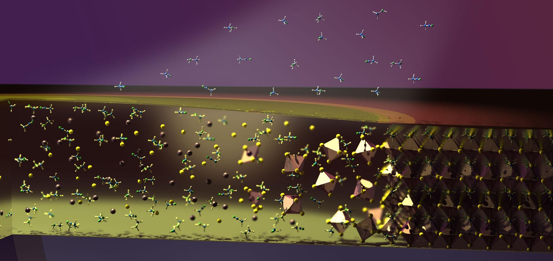
This roadmap provides a comprehensive overview of the latest advancements in lead-free perovskite materials for photovoltaic and photoelectrochemical /photocatalytic applications. It highlights the urgent need for sustainable energy solutions, emphasizing the role of lead-free perovskites in addressing challenges related to toxicity, scalability, and efficiency. The roadmap is designed to guide the reader from application-driven perspectives to fundamental materials insights, characterization techniques, fabrication strategies and overreaching sustainability considerations. The document explores key material families, including tin-, bismuth-, antimony-, and copper-based perovskites, detailing their optoelectronic properties, fabrication techniques, and application potential. Special attention is given to advanced characterization methods, green processing strategies, the integration of artificial intelligence and machine learning for material design and optimization and lifecycle impact assessments to ensure environmental sustainability. By bringing together insights from global research communities, this roadmap serves as a strategic guide for advancing lead-free perovskite technology, fostering interdisciplinary collaboration, and accelerating the transition to next-generation solar energy solutions.Impact of residual triphenylphosphine oxide on the crystallization of vapor-deposited metal halide perovskite films
Journal of Vacuum Science & Technology B Nanotechnology and Microelectronics Materials Processing Measurement and Phenomena American Vacuum Society 44:1 (2026) 012203
Abstract:
Thermal evaporation is an industrially compatible technique for fabricating metal halide perovskite thin films, without the requirement for hazardous solvents. It offers precise control over film thickness and is a good candidate for large-scale production of commercial optoelectronic metal halide perovskite devices, such as solar cells. The use of additives to passivate electronic defects in solution-processed metal halide perovskite has led to dramatic increases in device performance. However, there are a few reports of vapor-deposited films with coevaporated passivating agents. Triphenylphosphine oxide (TPPO) has been used as an effective surface passivating agent in solution-processed metal halide perovskite films. It is a promising candidate passivating agent for coevaporation, where it is beginning to be used with encouraging results. However, here we report that triphenylphosphine oxide is incompatible with thermal deposition in the same deposition chamber. Such TPPO remnants are found to result in severe suppression of the perovskite phase, long-range crystalline ordering, and optical absorption of lead halide perovskite films subsequently deposited in the same chamber. TPPO contamination persists even through repeated baking cycles, with the reduction of the contaminant to acceptable levels requiring vacuum chamber dismantling and manual cleaning. We conclude that TPPO should not be coevaporated in order to prevent the contamination of future batches.Tailoring a Lead-Free Organic–Inorganic Halobismuthate for Large Piezoelectric Effect
Journal of the American Chemical Society American Chemical Society 147:49 (2025) 45366-45376
Abstract:
Molecular piezoelectrics are a potentially disruptive technology, enabling a new generation of self-powered electronics that are flexible, high performing, and inherently low in toxicity. Although significant efforts have been made toward understanding their structural design by targeted manipulation of phase transition behavior, the resulting achievable piezoresponse has remained limited. In this work, we use a low-symmetry, zero-dimensional (0D) inorganic framework alongside a carefully selected ‘quasi-spherical’ organic cation to manipulate organic–inorganic interactions and thus form the hybrid, piezoelectric material [(CH3)3NCH2I]3Bi2I9. Using variable–temperature single crystal X-ray diffraction and solid-state nuclear magnetic resonance spectroscopy, we demonstrate that this material simultaneously exhibits an order–disorder and displacive symmetry-breaking phase transition. This phase transition is mediated by halogen bonding between the organic and inorganic frameworks and results in a large piezoelectric response, d 33 = 161.5 pm/V. This value represents a 4-fold improvement on previously reported halobismuthate piezoelectrics and is comparable to those of commercial inorganic piezoelectrics, thus offering a new pathway toward low-cost, low-toxicity mechanical energy harvesting and actuating devices.Impact of Halide Alloying on the Phase Segregation of Mixed‐Halide Perovskites
Small Structures Wiley (2025) e202500545